


Tutorial: Your FPGA Program: An LED Blinker
Part 2: Simulation of VHDL/Verilog
Simulation is a critical part of any design. It is very important to check that the code you wrote is behaving the way you expect it to behave. This is done with a simulator. The simulator that is most popular in the commercial world is called Modelsim and it is made by Mentor Graphics. Mentor graphics has a student version available. If you’ve never used Modelsim before, you can learn about how to use it by reading this Modelsim Tutorial for Beginners.
In order to simulate the design created previously, you need to create what is called a testbench. A testbench is code that exercises a design by observing the outputs of the design when the inputs are stimulated. Every design has expected behavior. In the LED Blinker code, we expect that the LED should light up at a different frequency based on the switch selections. The testbench allows us to pretend that we have real switches connected to our design. The testbench will allow us to toggle these switches and observe what happens to the output signal. If the output signal behaves the way you would expect, the test is a success. Let’s get started with our first testbench. There are two sections below, the first shows the VHDL Example, the second shows the Verilog Example.
Creating Your Testbench with VHDL
The first thing we need to do is to define the entity of the testbench. As a reminder, the entity contains all of the input signals and output signals. For a testbench, often there will be no input or output signals. All of the signals are generated internally to the testbench. Here’s the entity:
entity tutorial_led_blink_tb is
end tutorial_led_blink_tb;
That’s it. As a side note, _tb is a notation for testbench. So the entity name implies that this is a testbench for the entity tutorial_led_blink, which is the name of our design we are testing. Next is the architecture, signal declaration, and component declaration section. We have not yet discussed what a component is, so now is as good of a time as any.
“Component” is a keyword in VHDL that defines for the tools the nature of an entity somewhere in the design. It looks very similar to the entity that it matches. Here is the component for our design entity:
  component tutorial_led_blink is
    port (
      i_clock     : in  std_logic;
      i_enable    : in  std_logic;
      i_switch_1  : in  std_logic;
      i_switch_2  : in  std_logic;
      o_led_drive : out std_logic);
  end component tutorial_led_blink;
That tells the simulator that somewhere later in the file we will be using this entity. The actual use of the tutorial_led_blink entity comes when the entity is instantiated, which happens after the “begin” keyword. The instantiation is the piece of code that actually creates the design that we are testing. It serves an additional purpose: it creates a mapping of signals. Here is our instantiation:
  -- Instantiate the Unit Under Test (UUT)
  UUT : tutorial_led_blink
    port map (
      i_clock     => r_CLOCK,
      i_enable    => r_ENABLE,
      i_switch_1  => r_SWITCH_1,
      i_switch_2  => r_SWITCH_2,
      o_led_drive => w_LED_DRIVE
      );
You will notice that the => arrow is facing to the right. The signals to the left are the source signals, the signals to the right are the destination signals. Or if you prefer, the signals to the left are the signals in our design, the signals to the right are the signals in our testbench. If we stimulate the signals on the right, our LED Blinker design will react. The signals that will need to be stimulated are all of the inputs. The one output (w_LED_DRIVE) will not be stimulated. We will monitor that signal on the simulator to see if it is responding correctly to changes in input. Let’s start stimulating our inputs!
The first input we should consider is the i_clock input. Let’s create a signal called r_CLOCK that will have a 25 MHz clock. The p_CLK_GEN process in the code below creates the 25 MHz clock and will run continuously.
There is an additional process that contains the rest of the signals that we will be stimulating. Look at the code below and see how we are stimulating the signals r_ENABLE, r_SWITCH_1, and r_SWITCH_2. When this testbench and the design are compiled together, we are able to run the simulation. The specifics of how to compile and start your simulation are dependent on your simulator. You will need to look up some basic instructions on how to do this part on your own if you are not using Modelsim. Scroll down to see the testbench code and an output of the results of a simulation run.
tutorial_led_blink_tb.vhd:
library ieee;
use ieee.std_logic_1164.all;
use ieee.numeric_std.all;

entity tutorial_led_blink_tb is
end tutorial_led_blink_tb;

architecture behave of tutorial_led_blink_tb is

  -- 25 MHz = 40 nanoseconds period
  constant c_CLOCK_PERIOD : time := 40 ns;

  signal r_CLOCK     : std_logic := '0';
  signal r_ENABLE    : std_logic := '0';
  signal r_SWITCH_1  : std_logic := '0';
  signal r_SWITCH_2  : std_logic := '0';
  signal w_LED_DRIVE : std_logic;

  -- Component declaration for the Unit Under Test (UUT)
  component tutorial_led_blink is
    port (
      i_clock     : in  std_logic;
      i_enable    : in  std_logic;
      i_switch_1  : in  std_logic;
      i_switch_2  : in  std_logic;
      o_led_drive : out std_logic);
  end component tutorial_led_blink;

begin

  -- Instantiate the Unit Under Test (UUT)
  UUT : tutorial_led_blink
    port map (
      i_clock     => r_CLOCK,
      i_enable    => r_ENABLE,
      i_switch_1  => r_SWITCH_1,
      i_switch_2  => r_SWITCH_2,
      o_led_drive => w_LED_DRIVE
      );

  p_CLK_GEN : process is
  begin
    wait for c_CLOCK_PERIOD/2;
    r_CLOCK <= not r_CLOCK;
  end process p_CLK_GEN;

  process                               -- main testing
  begin
    r_ENABLE <= '1';

    r_SWITCH_1 <= '0';
    r_SWITCH_2 <= '0';
    wait for 0.2 sec;

    r_SWITCH_1 <= '0';
    r_SWITCH_2 <= '1';
    wait for 0.2 sec;

    r_SWITCH_1 <= '1';
    r_SWITCH_2 <= '0';
    wait for 0.5 sec;

    r_SWITCH_1 <= '1';
    r_SWITCH_2 <= '1';
    wait for 2 sec;

  end process;

end behave;
Creating Your Testbench with Verilog
First we should use the tick include `include compiler directive to include the Verilog code from Part 1 of this tutorial. The include keyword essentially inserts the entire contents of the tutorial_led_blink.v source file into the testbench source file. This makes it available for the testbench to use.
Secondly, we set simulation time units and precision time, which in this case is set to 1 μs and 1 ns respectively. The simulation time tells the simulator how often to update its values. It also sets the value of delay time units which are represented with the pound sign (#) AKA hashtag AKA octothorpe. So for example #1 would delay the simulator for 1 μs in our case. The precision time tells the simulator how to round its values. The thing to note here is that the larger the simulation time, the quicker your simulations will run. However if you are using a fast clock, you will need to set your simulation time to the nanosecond range.
`include "tutorial_led_blink.v"
`timescale 1us/1ns
Next we need to create the testbench itself, which will be called tutorial_led_blink_tb. Additionally let’s go ahead and define all of the signals that will be needed in this simulation.
module tutorial_led_blink_tb;

  reg r_CLOCK    = 1'b0;
  reg r_ENABLE   = 1'b0;
  reg r_SWITCH_1 = 1'b0;
  reg r_SWITCH_2 = 1'b0;

  wire w_LED_DRIVE;
Next we need to instantiate our LED Blinker so that the testbench can see it. The instantiation serves two purposes: two create the design, and to define the mapping of signals between the two modules. UUT is the name of our instantiation.
  // Instantiate the Unit Under Test (UUT)
  tutorial_led_blink UUT
    (
     .i_clock(r_CLOCK),
     .i_enable(r_ENABLE),
     .i_switch_1(r_SWITCH_1),
     .i_switch_2(r_SWITCH_2),
     .o_led_drive(w_LED_DRIVE)
     );
The signal after the dot are the signals in our UUT, the signals in the parenthesis are the signals in our testbench. For example: i_clock is the signal name in the UUT, r_CLOCK is the signal that is local to the testbench. If we stimulate the signals in the parenthesis, our LED Blinker design will react. The signals that will need to be stimulated are all of the inputs. The one output (w_LED_DRIVE) will not be stimulated. We will monitor that signal on the simulator to see if it is responding correctly to changes in input. Let’s start stimulating our inputs!
The first input we should consider is the i_clock input. Let’s create a signal called r_CLOCK that will have a 25 kHz clock. This can be done in one line of code as shown below. The #20 will delay for 20 μs before inverting the r_CLOCK signal (which is accomplished with the not ! operator).
always #20 r_CLOCK <= !r_CLOCK;
The remainder of the code is contained in a single initial block. Initial is a reserved keyword in Verilog that can only be used for simulation, it is not synthesized. It contains code that runs once and runs as soon as the simulation begins. In the initial block we toggle all of the input signals to check that our UUT is working as expected. Look at the code below and see how we are stimulating the signals r_ENABLE, r_SWITCH_1, and r_SWITCH_2. When this testbench and the design are compiled together, we are able to run the simulation. Below is the testbench code and an output of the results of a simulation run:
tutorial_led_blink_tb.v:
`include "tutorial_led_blink.v"
`timescale 1us/1ns

module tutorial_led_blink_tb;

  reg r_CLOCK    = 1'b0;
  reg r_ENABLE   = 1'b0;
  reg r_SWITCH_1 = 1'b0;
  reg r_SWITCH_2 = 1'b0;

  wire w_LED_DRIVE;

  // Instantiate the Unit Under Test (UUT)
  tutorial_led_blink UUT
    (
     .i_clock(r_CLOCK),
     .i_enable(r_ENABLE),
     .i_switch_1(r_SWITCH_1),
     .i_switch_2(r_SWITCH_2),
     .o_led_drive(w_LED_DRIVE)
     );

  always #20 r_CLOCK <= !r_CLOCK;

  initial begin
    r_ENABLE <= 1'b1;

    r_SWITCH_1 <= 1'b0;
    r_SWITCH_2 <= 1'b0;
    #200000 // 0.2 seconds

    r_SWITCH_1 <= 1'b0;
    r_SWITCH_2 <= 1'b1;
    #200000 // 0.2 seconds

    r_SWITCH_1 <= 1'b1;
    r_SWITCH_2 <= 1'b0;
    #500000 // 0.5 seconds

    r_SWITCH_1 <= 1'b1;
    r_SWITCH_2 <= 1'b1;
    #2000000 // 2 seconds

    $display("Test Complete");
  end

endmodule // tutorial_led_blink_tb
Results of Simulation
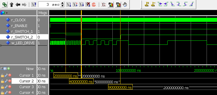
The yellow lines in the waveform view above represent changes to the r_SWITCH_1 and r_SWITCH_2 inputs. You can see that for the first 200 milliseconds of simulation time, the w_LED_DRIVE signal is toggling quickly, at 100 Hz. For the next 200 milliseconds, it toggles a bit slower, 50 Hz. Then it toggles at 10 Hz, and finally at 1 Hz. This waveform demonstrates that our design is coded correctly!
Congratulations, you have built and tested your first design!
This is the end of the beginner’s tutorial. You are on track to be a successful hardware designer! Feel free to browse around the Examples section to see how different pieces of code can be used.
Could someone explain why the first 2 lines of the Verilog testbench code have:
`include “tutorial_led_blink.v”
`timescale 1us/1ns
but these 2 lines don’t appear in the associated edaplayground Testbench for LED Blinker code that is linked to on the
nandland.com/project-6-how-to-simulate-your-fpga-designs
page?
Hi,
Excellent!
Thanks a lot.