Go Board – VGA Introduction
Learn how VGA works, display test patterns to your VGA monitor
VGA stands for Video Graphics Array and is a very common display interface. VGA was first introduced in 1987 and it is still widely supported today. Nearly 30 years for VGA’s prominence, very impressive! This project will get you acquainted with VGA and show you how the Go Board is able to drive your desktop monitor directly.
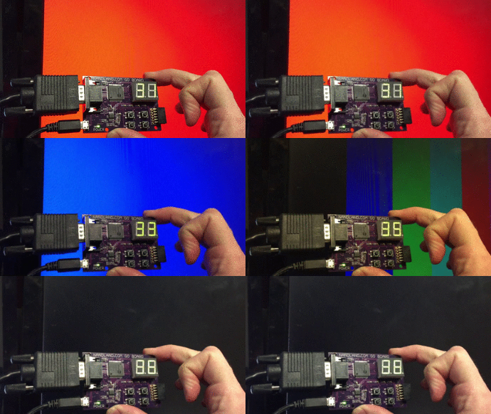
This is the goal outcome for this project:
Should you prefer to follow along with a YouTube video, well you can do that too! Please subscribe to my channel.
What is VGA? How Does it Work?
Today VGA is slowly being replaced by other displays such as DVI, HDMI, and DisplayPort to name a few. The reason that the Go Board uses VGA as
opposed to something like HDMI is that VGA is easier to deal with. The HDMI specification is very detailed, so interfacing directly from an FPGA to an HDMI display is more of a challenge than a VGA display. It’s best to learn the concepts about displays first using VGA.
The main difference between VGA and modern display interfaces is analog vs. digital. Analog means that the color driven to the pixel is determined by a voltage level. Digital means that the color driven to the pixel is determined by a binary code.
In addition to the analog voltage level, there’s some control signals, usually referred to as syncs that tell the monitor when to drive each pixel. These are Horizontal Sync and Vertical Sync. Let’s look at a single image frame.
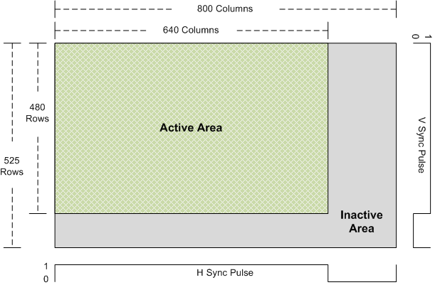
In the image above there is the green rectangle area which is the Active Area. This is the part of that frame that will actually be displayed on the monitor. When the image is displayed on the monitor, the pixels are actually displayed from left to right, top to bottom. Therefore, the top-left corner is the first pixel displayed and the bottom-right corner is the last pixel displayed. Because the pixels get displayed so quickly, the human eye is unable to see the it, and it looks like the entire image is drawn at once.
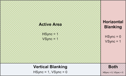
The two control signals H Sync and V Sync are also shown in the image above. HSync is high when you are in the active area of the frame horizontally. VSync is high when you are in the active area of the frame vertically. Therefore, if HSync and VSync are both high, then we are in the active area of the frame. If just HSync is high, then we are in the bottom inactive area of the frame. This is called the vertical blanking space. If just VSync is high, then we are in the horizontal blanking area of the frame. This is perhaps shown best in the image below:
For this project, we will be displaying video data at 60 Hz, meaning 60 frames per second. This project will be using an active area of 640 by 480, meaning 640 columns and 480 rows in the active area. There are a total of 794 columns and 525 rows in the total frame. This is a total of 794*525=416,850 pixels. Remember that the Go Board uses a 25 MHz clock. So if you draw one pixel per clock cycle, how much time does it take to draw an entire frame? 416850 / 25000000 = 0.01667 seconds. Remember that we are displaying frames at 60 Hz, and 1/60Hz = 0.01667 seconds per frame, so the math works! The total number of pixels in the frame allows us to draw one frame every 16.67 milliseconds. The main clock on the Go Board was specifically chosen to works well when driving a VGA display.
Now, it would be nice if all we had to do was drive HSync and VSync as shown in the image above. That would make the most sense. But unfortunately things aren’t that simple. Remember that originally VGA monitors were Cathode Ray Tubes (CRTs). Due to the way CRT displays work, we have to deal with the Front Porch and Back Porch. The front porch and back porch allow the active area to be shifted around your VGA monitor. You can think of them as modifications to your HSync and VSync pulses. For the Go Board, I show the times for each the front and back porch that work well. (Note that these values are modified slightly from here).
| VGA Timings using 25 MHz Clock | ||
|---|---|---|
| Line/Frame Part | Horizontal Pixels | Vertical Lines |
| Whole Area | 800 | 525 |
| Visible Area | 640 | 480 |
| Front Porch | 18 | 10 |
| Sync Pulse | 92 | 2 |
| Back Porch | 50 | 33 |
The timings above seem to work best for me. If you get better results with different values, please let everyone know in the comments below.
How Do Colors Work? Converting Digital Outputs to Analog
The Go Board does not have an analog output. Remember that VGA requires an analog voltage that represents the color value driven on the Red, Green, and Blue inputs. An analog voltage of 0.7 Volts represents full on for that particular color. So for example if you tie Red to 0.7 V, Blue to 0.0 V and Green to 0.0 V, then the monitor will display a purely red image (assuming you’re driving the Syncs correctly as well). The way the Go Board converts its digital outputs to an analog voltage is by a resistor divider. If you’re really interested in how this works, check out the schematic.
What you really need to know is that on the Go Board, each color (R, G, B) has 3-bits associated to it. This gives us a total of 512 possible colors. If you want to set the image to a pure red image, set the 3-bit RGB Outputs to 111, 000, and 000 respectively, for full red intensity. On the Go Board, bit 2 is the MSb, bit 0 is the LSb, so half Red intensity would be 100 for example.
Project Description
Create a project that outputs test patterns to the VGA port on the Go Board. The test patterns should be selectable by the computer keyboard. Use the UART and Binary-To-7-Segment modules from the previous project.
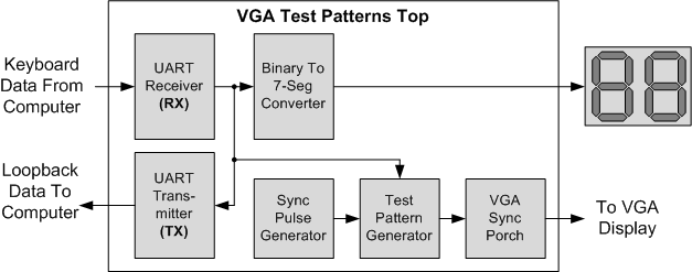
Look at the block diagram above. Now things are starting to get really interesting! We have a lot of modules that are all working together. The projects are building on each other to become more complicated and exercise more functionality on the FPGA. The code to drive the VGA display is linked in the EDA Playground environment below. The testbench only exercises the Sync Pulse Generator and the Test Pattern Generator. I included the necessary code for the VGA Front and Back Porch modifications in the EDA Playground for you. Once you have a handle on the VGA code, take a look at the top level module below to see how everything gets wired up. The results of the programmed Go Board are shown in the GIF below. I also included a short description of each of the new VGA modules in the block diagram.
Sync Pulse Generator:
The purpose of this module is to generate the sync pulses for the active and the inactive area using a 25 MHz clock. You should have some input parameters (in Verilog) or generics (in VHDL) that set the active and total number of rows and columns. This way, if the frame size changes, only the input values need to be updated. This module should simply generate free-running HSync and VSync that downstream modules can use to know where they are in the frame.
Test Pattern Generator:
The test pattern generator should be looking at where you are in your image based on the HSync and VSync inputs from the Sync Generator. Based on your location, you can keep a Column Counter and Row Counter. When you reach certain parts of the image, you can drive the pixel values differently, generating different colors. The actual test pattern that gets selected should be driven by some input to the module.
VGA Sync Porch:
This module modifies the sync pulses to add in the front and back porches required to properly drive the VGA display. The output of this module should the actual VGA signals that go right to the VGA pins.
Sync to Count:
Although this module is not shown in the block diagram above, I did add it to the EDA Playground environment. The purpose of this module is to simply output the Column and Row Index of the current pixel that we are on. This is useful information to know both in the Test Pattern Generator and in the VGA Sync Porch modules, so I chose to write the module once and instantiate it in two places. Reuse FTW.
VGA Test Pattern Code in Verilog
And now the top level code that instantiates everything:
VHDL Code – VGA_Test_Patterns_Top.vhd:
library ieee;
use ieee.std_logic_1164.all;

entity VGA_Test_Patterns_Top is
  port (
    -- Main Clock (25 MHz)
    i_Clk         : in std_logic;

    -- UART Data
    i_UART_RX : in  std_logic;
    o_UART_TX : out std_logic;

    -- Segment1 is upper digit, Segment2 is lower digit
    o_Segment1_A : out std_logic;
    o_Segment1_B : out std_logic;
    o_Segment1_C : out std_logic;
    o_Segment1_D : out std_logic;
    o_Segment1_E : out std_logic;
    o_Segment1_F : out std_logic;
    o_Segment1_G : out std_logic;

    o_Segment2_A : out std_logic;
    o_Segment2_B : out std_logic;
    o_Segment2_C : out std_logic;
    o_Segment2_D : out std_logic;
    o_Segment2_E : out std_logic;
    o_Segment2_F : out std_logic;
    o_Segment2_G : out std_logic;

	-- VGA
    o_VGA_HSync : out std_logic;
    o_VGA_VSync : out std_logic;
    o_VGA_Red_0 : out std_logic;
    o_VGA_Red_1 : out std_logic;
    o_VGA_Red_2 : out std_logic;
    o_VGA_Grn_0 : out std_logic;
    o_VGA_Grn_1 : out std_logic;
    o_VGA_Grn_2 : out std_logic;
    o_VGA_Blu_0 : out std_logic;
    o_VGA_Blu_1 : out std_logic;
    o_VGA_Blu_2 : out std_logic
    );
end entity VGA_Test_Patterns_Top;

architecture RTL of VGA_Test_Patterns_Top is

  signal w_RX_DV     : std_logic;
  signal w_RX_Byte   : std_logic_vector(7 downto 0);
  signal w_TX_Active : std_logic;
  signal w_TX_Serial : std_logic;

  signal w_Segment1_A, w_Segment2_A : std_logic;
  signal w_Segment1_B, w_Segment2_B : std_logic;
  signal w_Segment1_C, w_Segment2_C : std_logic;
  signal w_Segment1_D, w_Segment2_D : std_logic;
  signal w_Segment1_E, w_Segment2_E : std_logic;
  signal w_Segment1_F, w_Segment2_F : std_logic;
  signal w_Segment1_G, w_Segment2_G : std_logic;

  -- VGA Constants to set Frame Size
  constant c_VIDEO_WIDTH : integer := 3;
  constant c_TOTAL_COLS  : integer := 800;
  constant c_TOTAL_ROWS  : integer := 525;
  constant c_ACTIVE_COLS : integer := 640;
  constant c_ACTIVE_ROWS : integer := 480;

  signal r_TP_Index        : std_logic_vector(3 downto 0) := (others => '0');

  -- Common VGA Signals
  signal w_HSync_VGA       : std_logic;
  signal w_VSync_VGA       : std_logic;
  signal w_HSync_Porch     : std_logic;
  signal w_VSync_Porch     : std_logic;
  signal w_Red_Video_Porch : std_logic_vector(c_VIDEO_WIDTH-1 downto 0);
  signal w_Grn_Video_Porch : std_logic_vector(c_VIDEO_WIDTH-1 downto 0);
  signal w_Blu_Video_Porch : std_logic_vector(c_VIDEO_WIDTH-1 downto 0);

  -- VGA Test Pattern Signals
  signal w_HSync_TP     : std_logic;
  signal w_VSync_TP     : std_logic;
  signal w_Red_Video_TP : std_logic_vector(c_VIDEO_WIDTH-1 downto 0);
  signal w_Grn_Video_TP : std_logic_vector(c_VIDEO_WIDTH-1 downto 0);
  signal w_Blu_Video_TP : std_logic_vector(c_VIDEO_WIDTH-1 downto 0);

begin

  UART_RX_Inst : entity work.UART_RX
    generic map (
      g_CLKS_PER_BIT => 217)            -- 25,000,000 / 115,200
    port map (
      i_Clk       => i_Clk,
      i_RX_Serial => i_UART_RX,
      o_RX_DV     => w_RX_DV,
      o_RX_Byte   => w_RX_Byte);


  -- Creates a simple loopback to test TX and RX
  UART_TX_Inst : entity work.UART_TX
    generic map (
      g_CLKS_PER_BIT => 217)               -- 25,000,000 / 115,200 = 217
    port map (
      i_Clk       => i_Clk,
      i_TX_DV     => w_RX_DV,
      i_TX_Byte   => w_RX_Byte,
      o_TX_Active => w_TX_Active,
      o_TX_Serial => w_TX_Serial,
      o_TX_Done   => open
      );

  -- Drive UART line high when transmitter is not active
  o_UART_TX <= w_TX_Serial when w_TX_Active = '1' else '1';

  -- Binary to 7-Segment Converter for Upper Digit
  SevenSeg1_Inst : entity work.Binary_To_7Segment
    port map (
      i_Clk        => i_Clk,
      i_Binary_Num => w_RX_Byte(7 downto 4),
      o_Segment_A  => w_Segment1_A,
      o_Segment_B  => w_Segment1_B,
      o_Segment_C  => w_Segment1_C,
      o_Segment_D  => w_Segment1_D,
      o_Segment_E  => w_Segment1_E,
      o_Segment_F  => w_Segment1_F,
      o_Segment_G  => w_Segment1_G
      );

  o_Segment1_A <= not w_Segment1_A;
  o_Segment1_B <= not w_Segment1_B;
  o_Segment1_C <= not w_Segment1_C;
  o_Segment1_D <= not w_Segment1_D;
  o_Segment1_E <= not w_Segment1_E;
  o_Segment1_F <= not w_Segment1_F;
  o_Segment1_G <= not w_Segment1_G;

  -- Binary to 7-Segment Converter for Lower Digit
  SevenSeg2_Inst : entity work.Binary_To_7Segment
    port map (
      i_Clk        => i_Clk,
      i_Binary_Num => w_RX_Byte(3 downto 0),
      o_Segment_A  => w_Segment2_A,
      o_Segment_B  => w_Segment2_B,
      o_Segment_C  => w_Segment2_C,
      o_Segment_D  => w_Segment2_D,
      o_Segment_E  => w_Segment2_E,
      o_Segment_F  => w_Segment2_F,
      o_Segment_G  => w_Segment2_G
      );

  o_Segment2_A <= not w_Segment2_A;
  o_Segment2_B <= not w_Segment2_B;
  o_Segment2_C <= not w_Segment2_C;
  o_Segment2_D <= not w_Segment2_D;
  o_Segment2_E <= not w_Segment2_E;
  o_Segment2_F <= not w_Segment2_F;
  o_Segment2_G <= not w_Segment2_G;

  ------------------------------------------------------------------------------
  -- VGA Test Patterns
  ------------------------------------------------------------------------------
  -- Purpose: Register test pattern from UART when DV pulse is seen
  -- Only least significant 4 bits are needed from whole byte.
  p_TP_Index : process (i_Clk)
  begin
    if rising_edge(i_Clk) then
      if w_RX_DV = '1' then
        r_TP_Index <= w_RX_Byte(3 downto 0);
      end if;
     end if;
  end process p_TP_Index;

  VGA_Sync_Pulses_inst : entity work.VGA_Sync_Pulses
    generic map (
      g_TOTAL_COLS  => c_TOTAL_COLS,
      g_TOTAL_ROWS  => c_TOTAL_ROWS,
      g_ACTIVE_COLS => c_ACTIVE_COLS,
      g_ACTIVE_ROWS => c_ACTIVE_ROWS
      )
    port map (
      i_Clk       => i_Clk,
      o_HSync     => w_HSync_VGA,
      o_VSync     => w_VSync_VGA,
      o_Col_Count => open,
      o_Row_Count => open
      );

  Test_Pattern_Gen_inst : entity work.Test_Pattern_Gen
    generic map (
      g_Video_Width => c_VIDEO_WIDTH,
      g_TOTAL_COLS  => c_TOTAL_COLS,
      g_TOTAL_ROWS  => c_TOTAL_ROWS,
      g_ACTIVE_COLS => c_ACTIVE_COLS,
      g_ACTIVE_ROWS => c_ACTIVE_ROWS
      )
    port map (
      i_Clk       => i_Clk,
      i_Pattern   => r_TP_Index,
      i_HSync     => w_HSync_VGA,
      i_VSync     => w_VSync_VGA,
      --
      o_HSync     => w_HSync_TP,
      o_VSync     => w_VSync_TP,
      o_Red_Video => w_Red_Video_TP,
      o_Blu_Video => w_Blu_Video_TP,
      o_Grn_Video => w_Grn_Video_TP
      );

  VGA_Sync_Porch_Inst : entity work.VGA_Sync_Porch
    generic map (
      g_Video_Width => c_VIDEO_WIDTH,
      g_TOTAL_COLS  => c_TOTAL_COLS,
      g_TOTAL_ROWS  => c_TOTAL_ROWS,
      g_ACTIVE_COLS => c_ACTIVE_COLS,
      g_ACTIVE_ROWS => c_ACTIVE_ROWS
      )
    port map (
      i_Clk       => i_Clk,
      i_HSync     => w_HSync_VGA,
      i_VSync     => w_VSync_VGA,
      i_Red_Video => w_Red_Video_TP,
      i_Grn_Video => w_Blu_Video_TP,
      i_Blu_Video => w_Grn_Video_TP,
      --
      o_HSync     => w_HSync_Porch,
      o_VSync     => w_VSync_Porch,
      o_Red_Video => w_Red_Video_Porch,
      o_Grn_Video => w_Blu_Video_Porch,
      o_Blu_Video => w_Grn_Video_Porch
      );

  o_VGA_HSync <= w_HSync_Porch;
  o_VGA_VSync <= w_VSync_Porch;

  o_VGA_Red_0 <= w_Red_Video_Porch(0);
  o_VGA_Red_1 <= w_Red_Video_Porch(1);
  o_VGA_Red_2 <= w_Red_Video_Porch(2);

  o_VGA_Grn_0 <= w_Grn_Video_Porch(0);
  o_VGA_Grn_1 <= w_Grn_Video_Porch(1);
  o_VGA_Grn_2 <= w_Grn_Video_Porch(2);

  o_VGA_Blu_0 <= w_Blu_Video_Porch(0);
  o_VGA_Blu_1 <= w_Blu_Video_Porch(1);
  o_VGA_Blu_2 <= w_Blu_Video_Porch(2);

end architecture RTL;
Verilog Code – VGA_Test_Patterns_Top.v:
module VGA_Test_Patterns_Top
  (input  i_Clk,       // Main Clock
   input  i_UART_RX,   // UART RX Data
   output o_UART_TX,   // UART TX Data
   // Segment1 is upper digit, Segment2 is lower digit
   output o_Segment1_A,
   output o_Segment1_B,
   output o_Segment1_C,
   output o_Segment1_D,
   output o_Segment1_E,
   output o_Segment1_F,
   output o_Segment1_G,
   //
   output o_Segment2_A,
   output o_Segment2_B,
   output o_Segment2_C,
   output o_Segment2_D,
   output o_Segment2_E,
   output o_Segment2_F,
   output o_Segment2_G,

   // VGA
   output o_VGA_HSync,
   output o_VGA_VSync,
   output o_VGA_Red_0,
   output o_VGA_Red_1,
   output o_VGA_Red_2,
   output o_VGA_Grn_0,
   output o_VGA_Grn_1,
   output o_VGA_Grn_2,
   output o_VGA_Blu_0,
   output o_VGA_Blu_1,
   output o_VGA_Blu_2
   );

  // VGA Constants to set Frame Size
  parameter c_VIDEO_WIDTH = 3;
  parameter c_TOTAL_COLS  = 800;
  parameter c_TOTAL_ROWS  = 525;
  parameter c_ACTIVE_COLS = 640;
  parameter c_ACTIVE_ROWS = 480;

  wire w_RX_DV;
  wire [7:0] w_RX_Byte;
  wire w_TX_Active, w_TX_Serial;

  wire w_Segment1_A, w_Segment2_A;
  wire w_Segment1_B, w_Segment2_B;
  wire w_Segment1_C, w_Segment2_C;
  wire w_Segment1_D, w_Segment2_D;
  wire w_Segment1_E, w_Segment2_E;
  wire w_Segment1_F, w_Segment2_F;
  wire w_Segment1_G, w_Segment2_G;

  reg [3:0] r_TP_Index = 0;

  // Common VGA Signals
  wire [c_VIDEO_WIDTH-1:0] w_Red_Video_TP, w_Red_Video_Porch;
  wire [c_VIDEO_WIDTH-1:0] w_Grn_Video_TP, w_Grn_Video_Porch;
  wire [c_VIDEO_WIDTH-1:0] w_Blu_Video_TP, w_Blu_Video_Porch;

  // 25,000,000 / 115,200 = 217
  UART_RX #(.CLKS_PER_BIT(217)) UART_RX_Inst
  (.i_Clock(i_Clk),
   .i_RX_Serial(i_UART_RX),
   .o_RX_DV(w_RX_DV),
   .o_RX_Byte(w_RX_Byte));

  UART_TX #(.CLKS_PER_BIT(217)) UART_TX_Inst
  (.i_Clock(i_Clk),
   .i_TX_DV(w_RX_DV),      // Pass RX to TX module for loopback
   .i_TX_Byte(w_RX_Byte),  // Pass RX to TX module for loopback
   .o_TX_Active(w_TX_Active),
   .o_TX_Serial(w_TX_Serial),
   .o_TX_Done());

  // Drive UART line high when transmitter is not active
  assign o_UART_TX = w_TX_Active ? w_TX_Serial : 1'b1;


  // Binary to 7-Segment Converter for Upper Digit
  Binary_To_7Segment SevenSeg1_Inst
  (.i_Clk(i_Clk),
   .i_Binary_Num(w_RX_Byte[7:4]),
   .o_Segment_A(w_Segment1_A),
   .o_Segment_B(w_Segment1_B),
   .o_Segment_C(w_Segment1_C),
   .o_Segment_D(w_Segment1_D),
   .o_Segment_E(w_Segment1_E),
   .o_Segment_F(w_Segment1_F),
   .o_Segment_G(w_Segment1_G));

  assign o_Segment1_A = ~w_Segment1_A;
  assign o_Segment1_B = ~w_Segment1_B;
  assign o_Segment1_C = ~w_Segment1_C;
  assign o_Segment1_D = ~w_Segment1_D;
  assign o_Segment1_E = ~w_Segment1_E;
  assign o_Segment1_F = ~w_Segment1_F;
  assign o_Segment1_G = ~w_Segment1_G;


  // Binary to 7-Segment Converter for Lower Digit
  Binary_To_7Segment SevenSeg2_Inst
  (.i_Clk(i_Clk),
   .i_Binary_Num(w_RX_Byte[3:0]),
   .o_Segment_A(w_Segment2_A),
   .o_Segment_B(w_Segment2_B),
   .o_Segment_C(w_Segment2_C),
   .o_Segment_D(w_Segment2_D),
   .o_Segment_E(w_Segment2_E),
   .o_Segment_F(w_Segment2_F),
   .o_Segment_G(w_Segment2_G));

  assign o_Segment2_A = ~w_Segment2_A;
  assign o_Segment2_B = ~w_Segment2_B;
  assign o_Segment2_C = ~w_Segment2_C;
  assign o_Segment2_D = ~w_Segment2_D;
  assign o_Segment2_E = ~w_Segment2_E;
  assign o_Segment2_F = ~w_Segment2_F;
  assign o_Segment2_G = ~w_Segment2_G;

  //////////////////////////////////////////////////////////////////
  // VGA Test Patterns
  //////////////////////////////////////////////////////////////////
  // Purpose: Register test pattern from UART when DV pulse is seen
  // Only least significant 4 bits are needed from whole byte.
  always @(posedge i_Clk)
  begin
    if (w_RX_DV == 1'b1)
      r_TP_Index <= w_RX_Byte[3:0];
  end

  // Generates Sync Pulses to run VGA
  VGA_Sync_Pulses #(.TOTAL_COLS(c_TOTAL_COLS),
                    .TOTAL_ROWS(c_TOTAL_ROWS),
                    .ACTIVE_COLS(c_ACTIVE_COLS),
                    .ACTIVE_ROWS(c_ACTIVE_ROWS))
  VGA_Sync_Pulses_Inst
  (.i_Clk(i_Clk),
   .o_HSync(w_HSync_Start),
   .o_VSync(w_VSync_Start),
   .o_Col_Count(),
   .o_Row_Count()
  );


  // Drives Red/Grn/Blue video - Test Pattern 5 (Color Bars)
  Test_Pattern_Gen  #(.VIDEO_WIDTH(c_VIDEO_WIDTH),
                      .TOTAL_COLS(c_TOTAL_COLS),
                      .TOTAL_ROWS(c_TOTAL_ROWS),
                      .ACTIVE_COLS(c_ACTIVE_COLS),
                      .ACTIVE_ROWS(c_ACTIVE_ROWS))
  Test_Pattern_Gen_Inst
   (.i_Clk(i_Clk),
    .i_Pattern(r_TP_Index),
    .i_HSync(w_HSync_Start),
    .i_VSync(w_VSync_Start),
    .o_HSync(w_HSync_TP),
    .o_VSync(w_VSync_TP),
    .o_Red_Video(w_Red_Video_TP),
    .o_Grn_Video(w_Grn_Video_TP),
    .o_Blu_Video(w_Blu_Video_TP));

  VGA_Sync_Porch  #(.VIDEO_WIDTH(c_VIDEO_WIDTH),
                    .TOTAL_COLS(c_TOTAL_COLS),
                    .TOTAL_ROWS(c_TOTAL_ROWS),
                    .ACTIVE_COLS(c_ACTIVE_COLS),
                    .ACTIVE_ROWS(c_ACTIVE_ROWS))
  VGA_Sync_Porch_Inst
   (.i_Clk(i_Clk),
    .i_HSync(w_HSync_TP),
    .i_VSync(w_VSync_TP),
    .i_Red_Video(w_Red_Video_TP),
    .i_Grn_Video(w_Grn_Video_TP),
    .i_Blu_Video(w_Blu_Video_TP),
    .o_HSync(w_HSync_Porch),
    .o_VSync(w_VSync_Porch),
    .o_Red_Video(w_Red_Video_Porch),
    .o_Grn_Video(w_Grn_Video_Porch),
    .o_Blu_Video(w_Blu_Video_Porch));

  assign o_VGA_HSync = w_HSync_Porch;
  assign o_VGA_VSync = w_VSync_Porch;

  assign o_VGA_Red_0 = w_Red_Video_Porch[0];
  assign o_VGA_Red_1 = w_Red_Video_Porch[1];
  assign o_VGA_Red_2 = w_Red_Video_Porch[2];

  assign o_VGA_Grn_0 = w_Grn_Video_Porch[0];
  assign o_VGA_Grn_1 = w_Grn_Video_Porch[1];
  assign o_VGA_Grn_2 = w_Grn_Video_Porch[2];

  assign o_VGA_Blu_0 = w_Blu_Video_Porch[0];
  assign o_VGA_Blu_1 = w_Blu_Video_Porch[1];
  assign o_VGA_Blu_2 = w_Blu_Video_Porch[2];

endmodule
Now after building the code in iCEcube2, we should take a quick look at the synthesis results. How many LUTs and Registers (Flip-Flops) does your design use? Let’s take a look at the programmed Go Board in action.


[…] decided to deviate from the standard VGA tutorial on Nandland. Instead of following it, I only referred to the VGA overview and constants. The tutorial on […]