What is a Block RAM (BRAM) in an FPGA? Tutorial for beginners
They’re used for FIFOs, Dual Port Memories, and More!
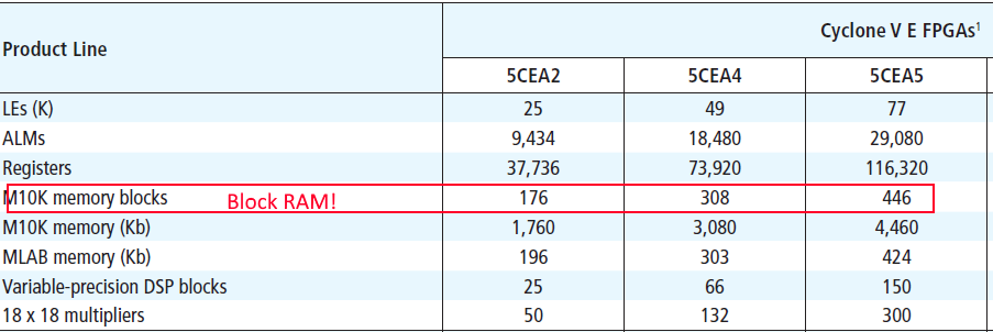
Block RAMs (or BRAM) stands for Block Random Access Memory. Block RAMs are used for storing large amounts of data inside of your FPGA. They one of four commonly identified components on an FPGA datasheet. The other three are Flip-Flops, Look-Up Tables (LUTs), and Digital Signal Processors (DSPs). Usually the bigger and more expensive the FPGA, the more Block RAM it will have on it. Since this is found right at the top of an FPGA product overview, it must be important! As an example, the image below shows the Product overview line comparing different Intel Cyclone V FPGAs.
A Block RAM (sometimes called embedded memory, or Embedded Block RAM (EBR)), is a discrete part of an FPGA, meaning there are only so many of them available on the chip. Each FPGA has a different amount, so depending on your application you may need more or less Block RAM. Knowing how much you will need gets easier as you become a better Digital Designer. As I said before, it’s used to store “large” amounts of data inside of your FPGA. It’s also possible to store data outside of your FPGA, but that would be done with a device like an SRAM, DRAM, EPROM, SD Card, etc.
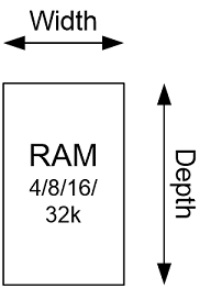
Block RAMs come in a finite size, 4/8/16/32 kb (kilobits) are common. They have a customizable width and depth. And they’re really useful for lots of applications! Let’s discuss some places where you might find yourself needing to create a Block RAM storage element for your project. Also, if you feel like watching the video version of this content I included that below.
Single Port BRAM Configuration
The Single Port Block RAM configuration is useful when there is just one interface that needs to retrieve data. This is also the simplest configuration and is useful for some applications. One example would be storing Read-Only Data that is written to a fixed value when the FPGA is programmed. That’s one thing about Block RAM, is that they can all be initialized (exception here is Microsemi FPGAs, which cannot be initialized because they’re a different architecture, but don’t worry about that!).
Maybe your application has a bunch of Calibration parameters that are written once and read out during boot, well a Single Port Block RAM would do the trick very well! Or maybe you need to do 8B/10B encoding/decoding, which is used commonly in Ethernet, HDMI, SATA, USB, etc. These would be great applications for single port Block RAMs.
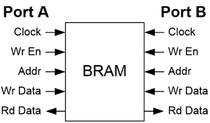
The way they work is all based on a Clock. Data will be read out on the positive edge of the clock cycle at the address specified by Addr as long as Wr En signal is not active. Read values come out on Rd Data, this is the data stored in the BRAM. Note that you can only read one Rd Data value per clock cycle. So if your Block RAM is 1024 values deep, it will take at least 1024 clock cycles to read the entire thing out.
There might be an application where you want to write some data into the Block RAM buffer, then read it out at a later time. This would involve driving Wr En high for one clock cycle and Wr Data would have your write data. For the single port configuration, you can either read or write data on Port A, you can’t do both at the same time. If you want to read and write data at the same time, you will need a Dual Port Block RAM!
Dual Port BRAM Configuration
The Dual Port Block RAM (or DPRAM) configuration behaves exactly the same way as the single port configuration, except you have another port available for reading and writing data. Both Port A and Port B behave exactly the same. Port A can perform a read on Address 0 on the same clock cycle that Port B is writing to address 200. Therefore a DPRAM is able to perform a write on one address while reading from a completely different address. I personally find that I have more use cases for DPRAMs than I do for Single-Port RAMs.
One possible use case would be storing data off of an external device. For example you want to read data off an SD Card, you could store it in a Dual Port RAM, then read it out later. Or maybe you want to interface to an Analog to Digital Converter (ADC) and will need some place to store the converted ADC values. A DPRAM would be great for this. Additionally, Dual Port RAMs are commonly turned into FIFOs, which are probably one of the most common use-cases for Block RAM on an FPGA.
FIFO BRAM Configuration
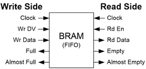
FIFO means First In First Out and they are used all over the place in FPGA design. Any time you need to buffer some data between two interfaces you’ll use a FIFO. Or if you want to cross clock domains, or if you want to buffer a row of image data and manipulate it, or if you want to send data off-chip to a DDR memory, these all require the use of a Block RAM FIFO.
FIFOs are so important to understand that I wrote an entire article just about them. They’re really fundamental in FPGA building, so I recommend checking that out.
How to create a Block RAM in VHDL or Verilog
So you want to actually create a Block RAM? Great! You have a few choices for how to proceed.
- Use Interactive GUI in Vivado, Quartus, Diamond, Libero, etc. I recommend this method for beginners to see how things work. This method is great to get comfortable with BRAM, but it can fall apart for large designs. The reason is that if each memory needs to be individually created, the GUI tool needs to be run many times and it becomes a burden on the FPGA designer.
- Infer a BRAM by creating a large memory in VHDL or Verilog. I am working on the GitHub code for this and will link to it when I am done. In the mean time, if you google “Infer Block RAM VHDL/Verilog” and whatever FPGA family you’re using you should find out how to do this.
- Use instantiation in VHDL or Verilog. A lot of times, you can instantiate the actual primitive for your particular FPGA. You need to refer to the Memory User’s Guide for details on how this works. One nice thing about this is that you know exactly what you’re getting when you directly instantiate the primitive. If you do this, I recommend writing a wrapper around it so that if you change FPGAs your main code does not have to change, just the wrapper file. And if you have no idea what I’m talking about then I don’t recommend this method for beginners.


I think the content here is more in line with Xilinx than the Intel FPGAs. For example, the defined size of a memory Block in Intel FPGAs is 10K as indicated by M10K Blocks. For inferring RAMs, if you declare the type as “ram” and declare the signal with this type, Quartus detects it as Memory. I am not sure about other FPGA manufacturers though.
A nice explanation for getting a good overview!. Thank you
Does anyone know the size of the Go Board BRAM?
It does not have BRAM, as it is introductory board.
The Go Board does in fact have Block RAM (BRAM). There is a total of 64 kbits available on the FPGA.
There is a total of 64 kbits of Embedded Block RAM available on the Go Board.